
Auger Electron Spectroscopy (AES) is a surface characterization technique used to identify the elemental composition of the outermost few nanometers of a material. For medical device manufacturing, this matters because many product failures, contamination issues, coating problems, corrosion behaviors, and adhesion challenges begin at the surface.
In the context of Costa Rica’s growing MedTech ecosystem, AES is relevant for companies working with precision components, implantable devices, coatings, polymers, metals, electronics, sensors, and clean manufacturing processes. It provides a way to investigate what is actually present on a surface—not just what the material specification says should be there.
Why surface chemistry matters in MedTech
Medical devices interact with demanding environments: biological fluids, sterilization processes, adhesives, coatings, packaging systems, electronic assemblies, and tightly controlled manufacturing lines. A small amount of surface contamination or an unexpected interfacial layer can influence:
- Coating adhesion
- Corrosion resistance
- Biocompatibility
- Electrical performance
- Bonding and joining quality
- Sterilization compatibility
- Root-cause analysis during failure investigations
- Supplier and process qualification
AES is especially useful when the question is:
What is present on the top few nanometers of this surface, and how does it change across an interface or contaminated region?
What AES measures
AES detects Auger electrons, which are emitted from atoms after they are excited by a high-energy incident electron beam. The energy of the emitted Auger electron is characteristic of the element that produced it, so AES can be used as an elemental fingerprint.
Because Auger electrons escape only from the very top region of a solid, AES is highly surface-sensitive. The useful signal typically comes from approximately:
1–5 nm from the surface
That makes AES valuable for identifying very thin surface films, residues, oxides, and contamination layers that may be invisible to bulk analysis methods.
How Auger electron emission works

Auger emission is a three-electron process:
- Core electron ejection A primary electron, typically with energy around
3–5 keV, strikes an atom and removes a tightly bound core electron. - Vacancy filling An electron from a higher shell falls into the vacancy left behind.
- Auger electron emission Instead of releasing the excess energy as an X-ray, the atom transfers that energy to another electron, which is emitted as an Auger electron.
The emitted electron has an energy that depends on the atom’s electronic structure. This is what allows AES to identify elements at the surface.
What elements can AES detect?

Because AES requires three electrons, it cannot analyze hydrogen or helium. For most other elements, AES is broadly applicable:
AES can detect elements with atomic number Z ≥ 3
Typical Auger electron energies fall in the range:
30–3000 eV
For example, silicon has important Auger transitions such as:
Si LVV ≈ 100 eVSi KLL ≈ 1.6 keV
These transitions can help identify whether silicon is present and, in some cases, whether its local bonding environment has changed.
Why AES requires ultra-high vacuum
AES analyzes only the top few nanometers of a surface. That strength also creates a challenge: the surface must remain clean during analysis.
If water vapor, oxygen, nitrogen, hydrocarbons, or other residual gases adsorb onto the sample, AES may detect those contaminants rather than the original surface. For that reason, AES systems typically operate under ultra-high vacuum, often around:
10⁻¹⁰ to 10⁻¹² torr
This vacuum requirement makes AES more complex and expensive than many routine inspection techniques, but it is essential for reliable surface analysis.
AES instrumentation in simple terms
A typical AES system includes:
- Electron source: Generates the primary beam that excites the sample.
- Ultra-high vacuum chamber: Keeps the surface clean during analysis.
- Electron energy analyzer: Measures the energies of emitted electrons.
- Detector: Counts electrons at selected energies.
- Scanning capability: Enables elemental surface maps.
- Optional sputter source: Removes material layer by layer for depth profiling.
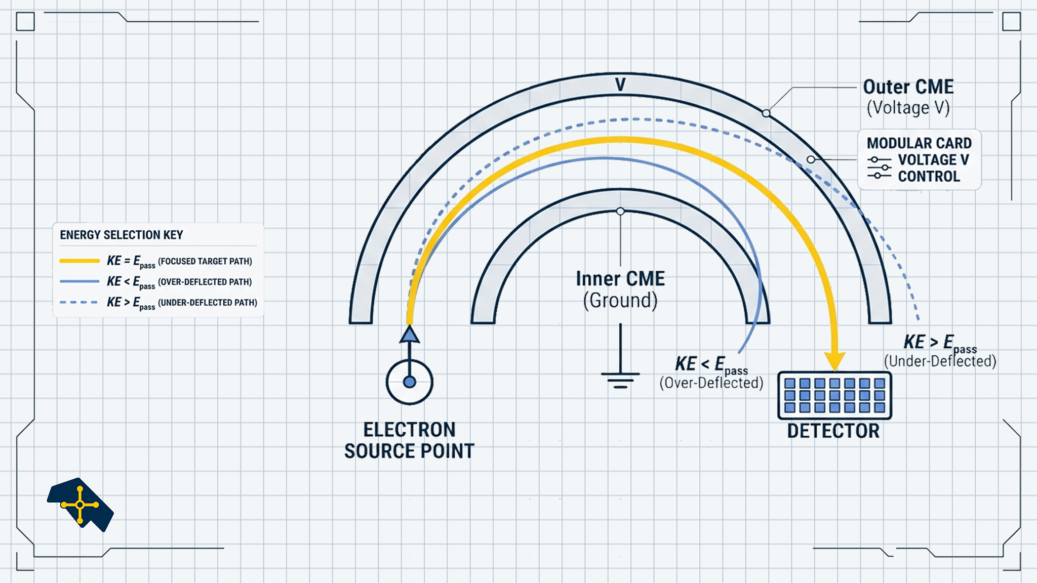
A common analyzer used in AES is the Cylindrical Mirror Analyzer (CMA). The CMA filters electrons by energy. By sweeping the analyzer voltage, the system counts electrons across an energy range and builds an Auger spectrum.

Reading an Auger spectrum
An Auger spectrum shows electron signal as a function of electron energy. Peaks in the spectrum correspond to elements present on the surface.
AES spectra may be displayed as:
N(E): electron counts as a function of energyE × N(E): energy-weighted electron yield- Differential spectra, such as
dN(E)/dE, which help highlight subtle peaks and changes
In practical failure analysis, the spectrum is compared with known reference libraries to identify the elements present.
Depth profiling: looking through thin layers
AES is naturally surface-sensitive, but it can be combined with ion sputtering to analyze composition as a function of depth.
In sputter depth profiling:
- AES measures the current surface.
- An inert ion beam, often argon, removes a very thin layer.
- AES measures the newly exposed surface.
- The process repeats.
This can reveal how composition changes through:
- Oxides
- Coatings
- Adhesion layers
- Thin films
- Interfaces
- Multilayer device structures
For example, AES can analyze a Si/SiO₂ interface. As sputtering removes the oxide, the oxygen signal decreases and the silicon signal changes as the analysis transitions from silicon dioxide to bulk silicon. In one example, the oxide thickness was approximately:
Tox ≈ 14.8 nm
This type of analysis is relevant to electronic medical devices, sensors, metallized components, and microfabricated structures.
Surface mapping: turning chemistry into an image
AES can also be used for elemental surface mapping. Instead of only collecting a standard SEM image, the system records the Auger signal for selected elements while scanning the electron beam across the surface.
This produces chemical maps that show where specific elements are concentrated.
Example: alloy and steel surfaces
A regular SEM image may show a dark region or contrast variation without explaining the cause. AES mapping can reveal whether that region corresponds to:
- Reduced iron concentration
- Increased oxygen concentration
- Manganese or boron segregation
- Oxide-rich regions
- Localized contamination
This matters for MedTech because metals and alloys are widely used in surgical tools, implants, needles, guidewires, hypotubes, and precision components. Local chemical variation can influence corrosion, passivation, fatigue, and surface performance.
Example: semiconductor and interconnect contamination
AES can also identify contamination in microelectronic structures. For example, in aluminum interconnects covered with titanium nitride, AES can distinguish:
- Aluminum
- Titanium nitride
- Silicon dioxide
- Carbon contamination
For medical electronics, wearables, diagnostics, sensors, and connected devices, this type of surface analysis can support failure analysis and process control.
Where AES fits in MedTech manufacturing
AES is not a routine incoming inspection tool for every component. It is a specialized technique used when surface-level chemical information is critical.
Potential MedTech use cases include:
- Failure analysis: Identifying unexpected surface residues, oxides, or contaminants.
- Coating investigations: Studying coating composition, interface quality, and adhesion-related issues.
- Metal surface analysis: Evaluating passivation, oxidation, alloy segregation, and contamination.
- Microelectronics and sensors: Investigating thin films, interconnects, and surface contamination.
- Supplier qualification: Verifying surface chemistry when material or process changes are suspected.
- Process development: Understanding how cleaning, plasma treatment, sterilization, or surface preparation affects a device.
- Interface analysis: Measuring composition changes across thin films, oxides, and bonding layers.
For Costa Rica’s MedTech sector, techniques like AES are part of the broader advanced characterization toolkit needed to support high-value manufacturing, process validation, and root-cause investigations.
Advantages of AES
AES offers several strengths for surface and interface analysis.
Strong surface sensitivity
AES focuses on the top few nanometers, making it excellent for contamination and surface chemistry studies.
Broad elemental coverage
AES can detect most elements except hydrogen and helium:
Z ≥ 3
Spatially resolved analysis
Modern AES systems can map features on the order of approximately 100 nm or smaller.
Depth profiling capability
When combined with sputtering, AES can show how elemental composition changes through coatings, oxides, and interfaces.
Useful reference libraries
AES has extensive reference spectra, which helps analysts compare measured spectra with known elemental signatures.
Mostly non-destructive without sputtering
If sputtering is not used, AES can be considered largely non-destructive because the sample is analyzed using an electron beam rather than physically sectioned or etched.
Limitations of AES
AES also has important limitations.
Limited sensitivity for trace concentrations
Because Auger emission is a three-electron process, the event probability is relatively low. AES is generally useful at concentrations around:
10¹⁹–10²⁰ atoms/cm³
This corresponds roughly to:
0.1–1 atomic %
That means AES is not usually the best choice for very low-level dopant analysis or trace impurity measurements.
Ultra-high vacuum requirement
AES requires complex ultra-high vacuum equipment. This makes the technique less accessible than routine microscopy or spectroscopy methods.
Sputtering is destructive
AES itself can be largely non-destructive, but sputter depth profiling removes material. Once sputtering begins, the surface has been physically altered.
Limited chemical bonding information
AES is primarily an elemental analysis technique. It can sometimes detect chemical shifts, such as differences between silicon in SiO₂ and bulk silicon, but it is not usually the strongest technique for detailed chemical bonding analysis.
Practical takeaway for MedTech teams
AES is most valuable when the problem is surface-specific and elemental in nature. It helps answer questions such as:
- Is there contamination on the surface?
- Which elements are present in a defect or residue?
- Does composition change across a coating or interface?
- Is an oxide, nitride, or carbon-rich layer present?
- Are alloying elements segregating to specific regions?
- Could a surface chemistry issue explain adhesion, corrosion, or electrical failure?
For MedTech manufacturers, AES can support investigations where nanometer-scale surface chemistry affects product performance, reliability, or manufacturability.
Summary
Auger Electron Spectroscopy is a powerful technique for analyzing the elemental composition of surfaces and interfaces. It uses characteristic Auger electrons generated by a three-electron atomic process, and it is especially sensitive to the top 1–5 nm of a material.
For the Costa Rica MedTech ecosystem, AES is relevant as an advanced characterization method for failure analysis, contamination control, coatings, metallic components, microelectronics, sensors, and thin-film interfaces. Its main trade-offs are the need for ultra-high vacuum, limited sensitivity for very low concentrations, and destructive analysis when sputtering is used.
In short, AES is not a general-purpose inspection method. It is a specialized, high-value tool for answering difficult surface chemistry questions when conventional SEM or bulk analysis is not enough.


Leave a Reply