
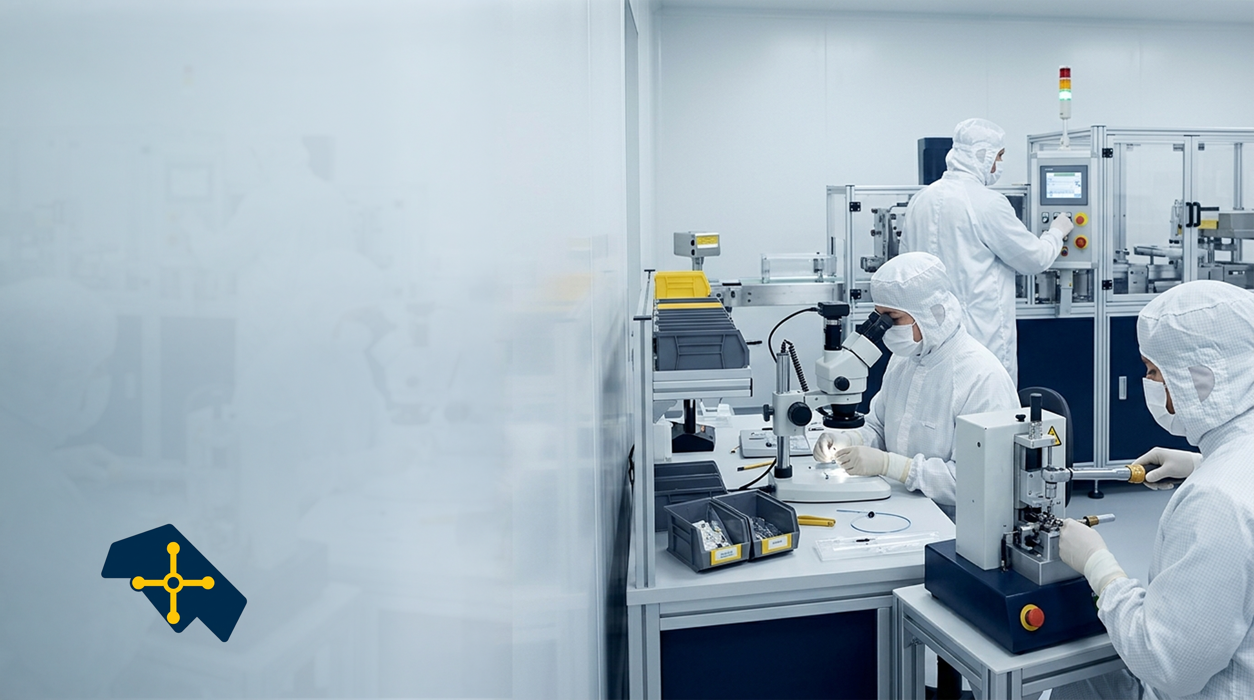
Semiconductors are one of those fields where materials science and electronics meet in the most practical way: what a material is (and how clean, ordered, and intentionally “imperfect” it can be made) ultimately determines what circuits can do.
I’m writing this series as an electronics engineer, and because earlier in my career I had the chance to work as an assistant professor to Dr.-Ing. Paola Vega at TEC. That experience pushed me to keep the “end-to-end story” in mind: it’s not just device physics, it’s also purification, crystal growth, surface finishing, thin films, and the unglamorous utilities (like ultrapure water) that make everything reliable.
This is why I’m starting the series on costaricamedtech.com. My goal is to connect the dots between the foundational materials/process story and the systems that depend on it. Especially MedTech, where success is less about chasing the smallest node and more about building reliable electronics, sensors, and evidence-backed manufacturing that hold up over long lifecycles.
In Costa Rica, that overlap is particularly relevant: we already have deep semiconductor-adjacent capability through Intel (design, manufacturing, and test), and the MedTech ecosystem increasingly intersects with cleanrooms, sensors, and microelectronics.
🧭TL;DR This post is a guided tour of how the industry goes from quartzite (SiO₂) → metallurgical silicon → ultra-pure chemistry → polysilicon → single-crystal ingots → polished wafers, and then into the films, conductors, cleaning chemistry, dopants, and utilities that make modern chips possible.
MedTech lens: a large fraction of MedTech value is created on mature, high-reliability electronics and MEMS + sensor stacks. Work where the winners are disciplined engineering teams that can design for manufacturability, characterize variation, and ship stable performance over long lifecycles.
In other words, the competitive advantage is often less about the smallest transistor and more about robust mixed-signal design, clean manufacturing execution, and evidence-backed test and reliability across years of production.
Before we start the process flow, a quick fundamentals anchor: from an electronics engineering perspective, materials in microfabrication fall into three buckets:
- Conductors (carry current easily)
- Insulators (block current)
- Semiconductors (can be engineered to conduct under some conditions and not under others)
In this article we concentrate on silicon, because the modern chip industry is largely built on silicon’s combination of abundance, extreme purifiability, and crystal quality.
✍️How to read this post – This is written like a guided walkthrough. Skim the headings first, then come back to the figures and tables as needed.
Table of Contents
It all starts with sand

Silicon’s industrial origin is sand / quartzite: silicon dioxide (SiO₂), i.e., oxidized silicon.
- Real-world sand can include many impurities (e.g., aluminum and other contaminants), and those impurities create downstream cost and performance limits.
- Some deposits are uniquely clean and therefore highly valuable. Spruce Pine, North Carolina, where a company sources the purest sand in the world is probably the most well known.
💡Key idea
At this point, the “story” looks deceptively simple: you have SiO₂ and you want Si. The catch is that oxygen is tightly bound to silicon, so the first real step is not mechanical, it’s chemical.
Silicon Step 1. Reduction
Because SiO₂ is silicon bonded to oxygen, the first major transformation is reduction: remove oxygen to obtain elemental silicon.
Submerged Electrode Furnace (SEF)

- Sand is loaded into a submerged electrode furnace (SEF).
- The furnace uses carbon electrodes and very high power (megawatts) to drive extreme temperatures.
- Heat alone doesn’t “solve” it; the goal is to drive the chemical reaction that strips oxygen.
- A carbon source is added. At high temperature:
- Carbon reacts with SiO₂, carrying oxygen away
- Products include silicon and exhaust gases such as CO and CO₂ (which are processed to be handled safely)
✅ Output (Step 1): metallurgical-grade silicon (MGS) at roughly ~98% purity. Metallurgical grade is good enough for alloying and related uses, but not nearly pure enough for electronics.
Silicon Step 2. Chemical Purification

Chemical refining: from MGS to ultra-pure silicon chemistry via repeated distillation.
MGS is still far from semiconductor grade. This is the pivot point where the process shifts from “melt and cast” thinking to chemical purification thinking.
Pulverize: MGS is crushed into fine powder to increase surface area. A common tool is a ball mill (a rotating container with hard media that grinds silicon down).
React with HCl: the powder reacts with HCl at around 300°C, forming chlorosilanes—most notably trichlorosilane (TCS, SiHCl₃).
Repeated distillation: this is where the purity jumps by orders of magnitude.
🧪Why distillation matters – Trichlorosilane can be repeatedly distilled (think: purification “passes”). Each pass knocks down trace contaminants further, pushing toward “9 nines” to “11 nines” purity.
- At device scales, parts-per-billion impurities can become yield- and reliability-limiting.
- SiHCl₃ purification target: 99.9999999%: “9 nines” to “11 nines.”
- Trace contaminants (iron, sodium, potassium, etc.) become decisive at device scales.
Silicon Step 3. Deposition

After purifying the silicon-bearing chemical, we convert it back into solid silicon.
Siemens process:
- Purified trichlorosilane is mixed with hydrogen and introduced into a chamber.
- The chamber has cooling around it so the vessel doesn’t fail thermally.
- The gas decomposes/condenses onto heated electrodes/rods, depositing high-purity polysilicon.
- The resulting silicon looks “weird” and is physically removed
Silicon Step 4. Crystal growth

Electronics-grade silicon is not only about purity; it must also have the right crystal structure. In other words: you can have very pure silicon and still have “the wrong silicon” for transistors if the lattice isn’t continuous.
Why single-crystal matters
For transistors to work properly, there is a quantum-mechanics-adjacent device requirement, silicon must be arranged in a regular crystal lattice across the wafer. Polysilicon (many crystals) is not sufficient for the main device substrate.
Czochralski (CZ) overview
🗣️Pronunciation: often just called “CZ”.
Process:
- Load high-purity polysilicon into a high-temperature, insulated chamber and melt it.
- Lower a seed crystal (already with the desired lattice orientation) into the melt.
- Rotate the seed one way and the crucible (kettle) the opposite way.
- The tip of the seed is slightly cooler; silicon freezes on it.
- Slowly pull upward (much slower than “demo videos”), continuing the crystal lattice and growing a single-crystal ingot.
- Temperature and pull rate control the neck/flare and final ingot diameter.
Process in video:
Doping during growth (baseline resistivity control)
During CZ growth, manufacturers can deliberately add small amounts of dopants (e.g., boron, phosphorus, sometimes arsenic) to set the wafer’s baseline resistivity “out of the box.”
- This is deliberate impurity; silicon without controlled impurity is not very useful electrically.
- There are also unavoidable trace impurities (e.g., oxygen contributions from the crucible) at very low levels.
📏Order-of-magnitude intuition
~10²³ silicon atoms per cm³
~10¹⁰ oxygen (atoms/units) per cm³ (dramatically lower than silicon)
Ingot into Wafers
Once a single-crystal ingot exists, turning it into wafers is a chain of mechanical + chemical steps:

Wafer-making sequence:
- Grow single-crystal ingot (CZ)
- Remove ends, machine diameter, add flat/notch for orientation
- Slice into wafers (wire saw)
- Stress-relief etch to remove surface damage
- Edge-grinding and CMP polishing (one or both sides)
Machining and orientation features (flats vs notch)
- Older/smaller wafers often have flats ground into the edge so humans/tools can determine orientation and doping type.
- Example described:
- 6-inch (150 mm) wafer can have two flats 90° apart for P-type doping (as an identification convention).
- For larger wafers (e.g., 200 mm / 8-inch, “small pizza pan”), a big flat wastes sellable area.
- Industry shifted toward a small notch so robotics can locate orientation while preserving wafer real estate.
Slicing with wire saw and why the surface is damaged
- Ingot is sliced using many wires (abrasive/diamond cutting effect).
- This wastes kerf material (captured and reused).
- The cut surfaces are rough and stressed; the wafer “wants to break” due to being a single crystal.
Lapping/polishing + chemical stress-relief etch + CMP
A typical flow:
- Lapping knocks down high spots on both sides
- A slurry is used (a base with small glass beads) to thin and smooth wafers
- Then a stress relief etch (chemical) removes subsurface damage using hydrofluoric acid in a base.
- Finally, CMP (chemical mechanical polish) achieves the mirror-like surface needed for thin films and lithography
- Often one side is polished to mirror quality; the backside may be smooth but not mirror-finished
Insulators & Conductors
In fabrication we build devices and interconnect stacks by repeating a pattern:
- Put down a material film
- Pattern it
- Remove what we don’t want
- Repeat across many layers
💡Key idea (scaling): as dimensions shrink, materials stop behaving “ideally.” Metals can begin to lose good conductor behavior at very small line widths; insulators can leak/break down at high fields and speeds. This forces the industry to switch materials over time.
Insulators: oxides, nitrides, high‑k dielectrics
Silicon dioxide (SiO₂, “oxide”)
- Can be grown directly on silicon in a furnace by flowing oxygen.
- This is powerful because the substrate itself becomes a high-quality insulator with comparatively simple processing.
Silicon nitride (Si₃N₄, “nitride”)
- Typically deposited (it doesn’t “grow” like oxide).
- It’s non-reactive like Teflon.
- Nitride can be used as a mask/barrier to control where oxide grows. This is critical because unpatterned films don’t accomplish much until you can pattern them.
Capacitance + Leakage
At high speeds and small dimensions:
- Two conductors separated by a dielectric behave like a capacitor.
- If fields/speeds are extreme, dielectrics can break down / leak, effectively shorting behavior.
- Meanwhile transistors want a high capacitance gate stack, but interconnect dielectrics often want low capacitance to reduce parasitics.

This is why advanced stacks introduce “exotic” dielectrics such as hafnium oxide:
- Enables high capacitance with very thin films where SiO₂ alone would leak too much.
Conductors: aluminum vs copper
Properties, tradeoffs, and the interconnect patterning revolution. There has been a long-running transition from aluminum to copper with new patterning technology.
| Property | Aluminum | Copper |
|---|---|---|
| Resistivity | 2.7 μΩ*cm | 1.7 μΩ*cm |
| Resistance to corrosion | Fair | Poor |
| Wet etchant | Phos/acetic/nitric (PAN) | Nitric |
| (Plasma) dry etchant | CCl4, CCl4 and Ar, BCl3 | None as of yet |
| Diffusion | Slow | Fast |
| Electromigration | Poor | Good |
| Cross contamination | Good | Poor |

Patterning aluminum (classic subtractive etch)
Simple three-step conceptual flow:
- Deposit aluminum film (it can fill contact holes reasonably well)
- Photolithography to define pattern
- Etch aluminum where not protected by photoresist (wet or dry), then strip resist
Outcome: aluminum remains only where desired (e.g., making contact to silicon but not shorting along an insulator).
Patterning copper (damascene: add + polish instead of etch)
Because copper can’t be plasma etched for fine features, the industry adopted damascene:
- Create trenches/vias in the dielectric (pattern the dielectric, not the copper)
- Deposit a thin copper seed/barrier layer
- Electroplate copper to fill features (bulk deposition alone is not efficient)
- Use CMP to polish away excess copper from the top surface
- Copper remains only in the trenches/vias
This adds complexity (including chemistry/plating constraints, contamination control, and tool segregation), but enables smaller lines—smaller lines → higher density → more value.
Why copper is attractive (and painful)
- Copper is more conductive (lower resistivity) → better for signal integrity and power.
- But copper:
- corrodes easily
- diffuses faster into silicon (process challenges during high-temperature steps)
- contaminates silicon more severely (cross-contamination risk)
- and most critically: there is no practical plasma etch for copper for fine patterning
Acids, bases, and solvents
Semiconductor fabrication is as much about removing material and contamination as it is about adding films. A lot of the “magic” in a fab is simply controlling what gets to touch the wafer, and when.
⚠️Key warning: if you heat a wafer (e.g., to grow oxide), contaminants can be driven into silicon. So cleaning before high-temperature steps is critical.
List of acid and bases used to etch or clean semiconductor materials
| Chemical | Typical use |
|---|---|
| Hydrochloric acid | Second part of RCA wafer clean |
| Hydrofluoric acid (HF) | Etches silica / SiO₂ |
| Phosphoric acid | Etches silicon nitride |
| Acetic acid | Mixed to etch aluminum, polysilicon |
| Sulfuric acid | Organic remover (piranha etch with peroxide) |
| Ammonium hydroxide | First part of RCA wafer clean |
| TMAH (2.6% in water) | Develops positive photoresist |
| Hydrogen peroxide (30%) | RCA wafer clean, piranha etch |
- HF etches glass/SiO₂ (useful for oxide removal).
- Phosphoric acid (heated, with controlled water) can etch nitride.
- RCA cleaning relies on mixtures involving ammonia/peroxide and HCl/peroxide.
- Piranha etch (sulfuric acid + peroxide) is an extremely aggressive organic remover.
- Popular misconceptions HF does not behave the way it’s often portrayed; piranha is the truly aggressive organic-dissolving chemistry.
- Core wafer-clean chemistries were developed decades ago (mid-20th century) and remain foundational because they work.
List of solvents used to dissolve materials away
| Chemical | Use |
|---|---|
| Acetone | Cleaning |
| Methanol | Cleaning |
| Isopropanol | Cleaning |
| Ethanol (infrequently used) | Cleaning |
| Propylene glycol methyl ether acetate (PGMEA) | Photoresist solvent |
| 1-methyl-2-pyrrolidinone (NMP) | Photoresist solvent/remover |
Dopants
Pure silicon is not very useful until we modify carrier concentration using dopants.
Valence-electron framing
- Silicon has 4 valence electrons.
- P-type dopants come from group III (e.g., boron, also aluminum).
- They have 3 valence electrons → effectively one “missing” electron → hole/positive-type behavior.
- N-type dopants come from group V (e.g., phosphorus, arsenic, sometimes antimony).
- They have 5 valence electrons → extra electron → negative-type behavior.

The p–n junction region is what enables key device behavior (transistors/diodes).
Applying dopants – diffusion methods (historical) vs ion implantation (modern standard)
Wafer doping (possible during CZ growth) is different from patterned doping used to form localized device regions (source/drain, etc.). Patterning requires the dopant to be applied selectively
Older diffusion-based methods (largely phased out since ~mid-1980s)
- Solid source diffusion
- B2O3 or P2O5 discs + diffusion furnace 620-660°C.
- Stack dopant-bearing wafers next to silicon wafers in a furnace.
- Dopant-bearing glass forms on the wafer surface.
- Then a long high-temperature drive-in (e.g., ~1000°C for a very long time up to 24hrs) diffuses dopant into silicon.
- Spin-on-glass diffusion
- Spin a dopant-containing liquid onto the wafer.
- Glass is applied, then furnaced at recommended temperature/time
- Glass is removed, doping driven in by furnace 1000°C up to 24 hrs
These approaches are diffusion-driven, with limited control over dose and depth.
Ion implantation (precise control)
Ion implantation solves control problems:
- Can effectively “count” ions implanted (dose control).
- Implant energy controls depth (how “hard” you shoot ions controls penetration).
- Tool is under vacuum to enable acceleration.
Implanter concept:
- A dopant-bearing gas is introduced into a source region and ionized.
- A magnet bends ions; bending radius depends on mass/charge, enabling mass selection (select the desired dopant species through an aperture, analogous to selecting a “color” from a spectrum).
- Then ions are accelerated through increasing electric potentials and implanted into the wafer.
☠️Safety note: many dopant gases are lethal if inhaled; tool and facility safety systems are non-negotiable.
Ultrapure / DI water (UPW): the quiet backbone of processing
Wafer processing requires rinsing/cleaning that does not add contamination. UPW/DI water systems remove particles, dissolved solids, and ions and often include continuous recirculation, UV, and fine filtration.
Used for rinsing can’t add any contamination. Remember that even the best filtered and processed city (tap) water contains a list of impurities:
- Na, K, Ca, Mg, Fe, and possibly traces of Pb, Zn, and Cu positive ions
- Cl, SO, NO3, CO3, HCO3 negative ions
- Some dissolved gases and possibly organics as well
That is why this multistage process is necessary. UPW is the “invisible material” in the fab. It is used everywhere, so any contamination in the rinse stream becomes contamination on the wafer. It enables continuous monitoring and re-polishing as needed (quality control is continuous, not “set-and-forget”).

1. Conditioning (protect the RO + stabilize the feed)
- Removes particles early (prefilter) so membranes and downstream components don’t foul.
- Removes hardness (softener) so scale doesn’t form on RO membranes and piping.
- Removes chlorine/chloramines (activated carbon) because oxidizers can damage RO membranes and can contribute to corrosion issues.
- Overall goal: make the incoming water predictable and “membrane-friendly”.
2. Reverse Osmosis (RO) (bulk purification
- Removes the majority of TDS (salts/minerals) and reduces organic load.
- Acts like a high-throughput “bulk filter” so the later polishing stages aren’t overloaded.
- Produces both a product stream (RO permeate) and a reject/brine stream (concentrated contaminants).
3. Deionizing (DI) / Mixed-bed polishing (ionic cleanup)
- Removes remaining ions using ion-exchange resins.
- This is what pushes water quality toward very high resistivity (often referenced as 18.2 MΩ·cm at 25°C).
- Why it matters: ions are electrically active contamination and can drive corrosion, mobile-ion effects, and reliability failures.
4. UV treatment + final 0.2 µm filtration (polish + protect point-of-use)
- UV helps control bioburden and breaks down some organics so they can be removed more effectively.
- The 0.2 µm final filter catches remaining particles and any biological fragments before water reaches the tools.
5. Recirculation (keep water clean after it’s made)
- Prevents stagnation (which can enable microbial growth and particle shedding).
- Keeps temperature/quality more uniform across the facility loop.
MedTech chips in Costa Rica
It’s easy to assume “semiconductors” means bleeding-edge nodes, smartphone volumes, and headline-grabbing fabs. In practice, a large fraction of MedTech value is created on mature, high-reliability electronics and MEMS + sensor stacks. Work where the winners are disciplined engineering teams that can design for manufacturability, characterize variation, and ship stable performance over long lifecycles.
In other words, the competitive advantage is often less about the smallest transistor and more about robust mixed-signal design, clean manufacturing execution, and evidence-backed test and reliability across years of production.

MedTech as a “mature-node” customer
If you zoom out, this is part of a broader “legacy chip” reality: mature-node semiconductors may not be glamorous, but they are essential to systems that must keep working in the real world, including medical equipment.
- Many medical products rely on microcontrollers, analog front ends, power management, and connectivity ICs where the priorities are long lifecycle availability, predictable behavior, and reliability, not the smallest transistor.
- This makes MedTech unusually sensitive to supply continuity and long-term component support. Shortages or end-of-life events can translate into redesign work, regulatory impact, and (in some cases) care disruption.
📚 Further Reading:
– The changing landscape of semiconductor manufacturing: why the health sector should care
– Investments in Semiconductor Chip Manufacturing Critical for Medtech Industry, Patient Health
– Latin America’s Role in De-Risking Semiconductor Supply Chains
MEMS + sensors

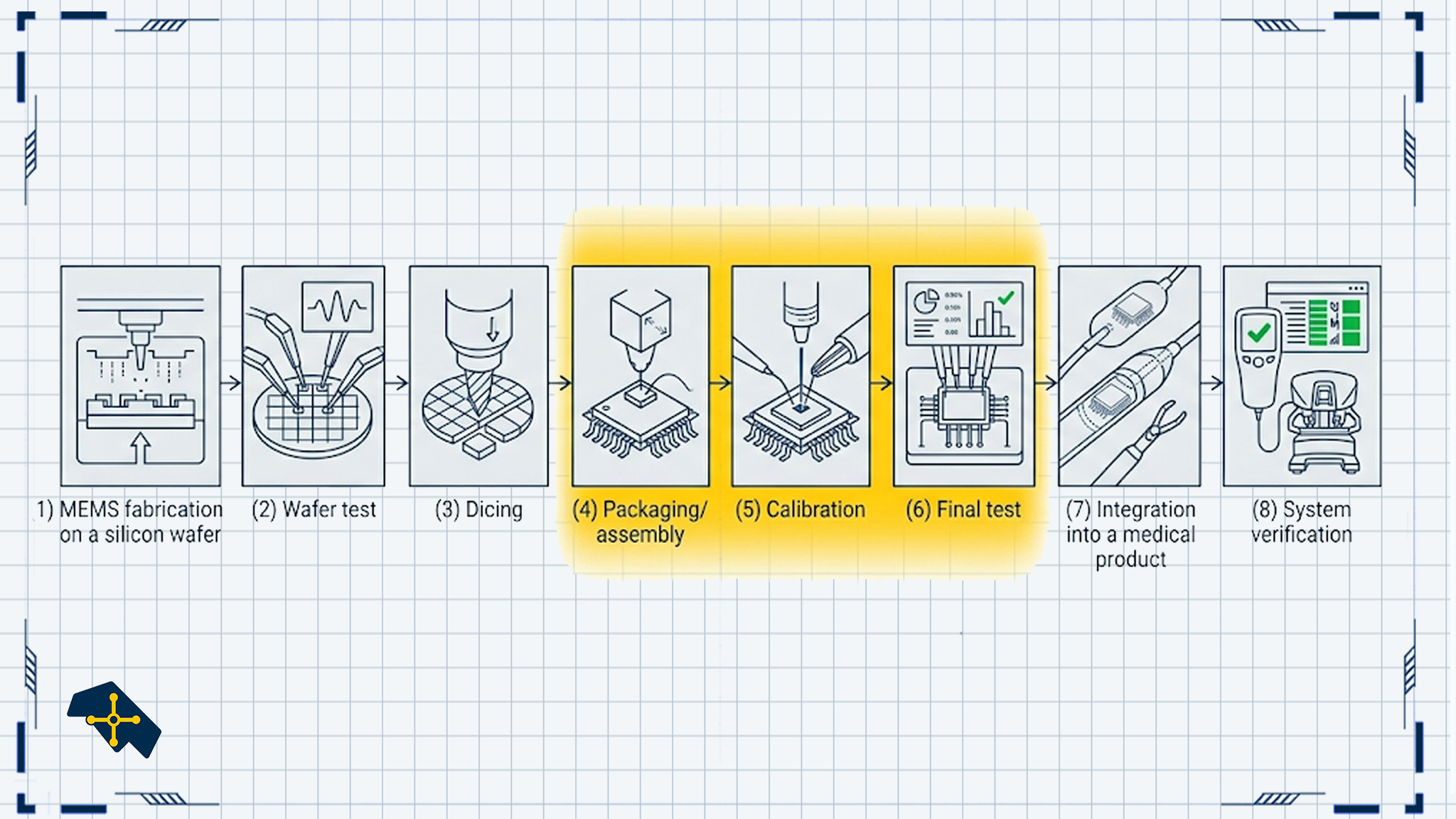
MEMS devices are built using wafer-scale microfabrication techniques, then packaged, calibrated, and tested into sensor products.
In healthcare that can mean pressure sensors, inertial sensing, lab-on-chip / microfluidic components, and other “electronics-meets-physics” building blocks that sit upstream of diagnostics and monitoring.
In practice, this is where semiconductor and MedTech manufacturing converge: you need clean manufacturing discipline, stable processes, and evidence-backed test strategies. Exactly the kind of “hands-on” operational learning costaricamedtech.com is trying to make visible and transferable.
This overlap is not hypothetical in Costa Rica: companies are explicitly investing in the country around sensor-driven medical devices that combine microelectronics, biosensors, and specialized sensing modalities.

“Costa Rica has taken a leap forward in the sophistication of the processes associated with medical device manufacturing. Evidence of this is that companies such as Forj Medical are setting up operations in the country to develop surgical navigation technologies, biosensors, and microelectronics; confirming the strength and diversity of a sector that now represents 48% of our goods exports and grew by nearly 30% through October of this year. Our talent, infrastructure, and ecosystem enable this industry to reach new levels of precision, innovation, and global reach.” – Laura López – CEO, Procomer 2025
📚 Further Reading:
– Microelectromechanical Systems (MEMS) for Biomedical Applications
– MEMS – Managing the full design and manufacturing chain
– Forj Medical – Primera compañía en el país dedicada a la fabricación de sensores electromagnéticos personalizados – Dic, 2025
Growth angle for Costa Rica
Costa Rica has a rare asset: decades of semiconductor-adjacent talent built through Intel across design center work, plus manufacturing and test disciplines. That combination matters because many of the hardest problems in MedTech electronics and sensors live at the interface of:
- design intent → verification → manufacturability
- packaging/assembly constraints → test strategy → quality/reliability evidence
- controlled change management across long product lifecycles
Bringing more companies that build MedTech electronics, sensors, and mature-node-dependent products can strengthen ecosystem resilience:
- Sustainability and stability: more diverse, higher-value technical employers with export-driven growth.
- Capability compounding: shared talent, suppliers, labs (calibration, reliability), and cross-industry learning.
- Upstream pull: demand for better packaging/test, precision manufacturing, and quality systems. These capabilities spill over into other regulated industries.

Key Takeaways
Shrinking features is not just “making things smaller.” It is an ongoing negotiation with physics and chemistry:
- Purity chemistry enables reliable semiconductor behavior.
- Crystal growth enables reproducible device physics.
- Mechanical + chemical finishing enables lithography-ready surfaces.
- Oxides/nitrides and advanced dielectrics keep capacitors and leakage under control.
- Metal choices and patterning constraints reshape interconnect technology (aluminum → copper → future materials).
- Cleaning chemistry and ultrapure water prevent “invisible” contamination from becoming device failure.
- Dopants and implantation enable controlled p–n structures at nanoscale.
- Purity and surfaces are not academic details: they drive leakage, reliability, and yield. Ultimately they drive whether electronics behave predictably.
- Modern silicon is a manufacturing story as much as a physics story: distillation, crystal growth, CMP, cleaning chemistry, and UPW are the hidden enablers.
- MedTech overlap is often “mature-node + mixed-signal + sensors,” not leading-edge nodes: lifecycle, reliability evidence, and supply continuity can dominate.
- MEMS turns microfabrication into sensing capability: the value is frequently at the interfaces (packaging, calibration, final test, and ongoing reliability).
- Costa Rica can compound capabilities by leveraging Intel-derived design/manufacturing/test talent to attract MedTech electronics and sensor work, building the labs and suppliers that make the ecosystem more resilient over time.
Shrinking features is not just “making things smaller.” It is an ongoing negotiation with physics and chemistry:
- Purity chemistry enables reliable semiconductor behavior.
- Crystal growth enables reproducible device physics.
- Mechanical + chemical finishing enables lithography-ready surfaces.
- Oxides/nitrides and advanced dielectrics keep capacitors and leakage under control.
- Metal choices and patterning constraints reshape interconnect technology (aluminum → copper → future materials).
- Cleaning chemistry and ultrapure water prevent “invisible” contamination from becoming device failure.
- Dopants and implantation enable controlled p–n structures at nanoscale.

In short: materials + process integration is what turns sand into chips, and scaling is ultimately limited (and enabled) by materials choices and the ability to deposit, pattern, clean, and connect them precisely.
Glossary
| Term | Meaning |
|---|---|
| Acceptor | A dopant atom (typically Group III in silicon) that “accepts” an electron, creating a hole and enabling p-type behavior. |
| Activated carbon filter | Water-treatment stage that removes chlorine/chloramines and many organics to protect downstream membranes and improve UPW quality. |
| Ball mill | A rotating mill with hard media that crushes metallurgical-grade silicon into a fine powder to increase surface area for chemical refining. |
| Brine / reject stream | The concentrated waste stream from reverse osmosis that carries away the rejected dissolved solids. |
| Capacitance (parasitic) | Unintended capacitor-like coupling between conductors separated by a dielectric; becomes more problematic as dimensions shrink. |
| Chlorosilane | A silicon-containing chemical (e.g., trichlorosilane) used as an intermediate for purification because it can be distilled to extremely high purity. |
| Conductors / insulators / semiconductors | The three broad material categories in microfabrication: good current carriers, current blockers, and materials whose conductivity can be engineered via doping and structure. |
| Cross-contamination | Unwanted transfer of materials (especially metals like copper) into tools or wafers that can degrade device performance or yield. |
| Damascene | Copper interconnect patterning approach: etch trenches/vias in dielectric, add barrier/seed, electroplate copper, then CMP away excess copper. |
| Design for manufacturability (DFM) | Engineering practice of designing products and processes so they can be manufactured and tested reliably at scale (yield, variation, and testability built in up front). |
| Dielectric | An insulating material used to separate conductors (e.g., between metal lines or in gate stacks), influencing capacitance and leakage. |
| Doping | Deliberate introduction of controlled impurity atoms to set carrier type and concentration (p-type or n-type) in silicon. |
| Electroplating | Electrochemical process used to deposit copper efficiently into damascene trenches/vias after a seed layer is present. |
| Etch (wet vs dry) | Material removal using liquid chemistry (wet) or plasma chemistry (dry); selectivity and pattern fidelity are key constraints. |
| High-k dielectric | A dielectric with high permittivity (e.g., hafnium oxide) that enables high capacitance with low leakage when SiO₂ would be too leaky at small thickness. |
| Ion implantation | Precise doping method where ions are accelerated under vacuum into the wafer to control dose and depth. |
| Kerf | Material lost as “sawdust” during wafer slicing (e.g., wire saw); often collected for recovery/reuse. |
| Lapping | Mechanical smoothing step after wafer slicing to remove high spots and help reduce surface damage before final polishing. |
| Leakage / breakdown | Non-ideal dielectric behavior where current leaks through or the insulator fails under high electric fields, worsened by scaling. |
| Legacy / mature-node (semiconductors) | Semiconductor process nodes and technologies that prioritize proven reliability, availability, and lifecycle stability (often used for analog, mixed-signal, power, and many embedded applications). |
| Metallurgical-grade silicon | ~98% pure silicon produced by reducing SiO₂ in a furnace; not yet pure enough for electronics. |
| Mixed-bed resin | A blend of cation/anion ion-exchange resins used in UPW systems to remove trace ions and reach very high resistivity. |
| Mixed-signal | Electronics that combine analog and digital functions (common in sensor front-ends, converters, and medical instrumentation). |
| Notch / flat (wafer orientation) | Mechanical features on wafer edges used by tools (and historically by humans) to identify orientation and sometimes doping conventions. |
| Polysilicon | Silicon made of many small crystals; used widely as a deposited film and as feedstock for single-crystal growth, but not used as the main wafer substrate. |
| Product change notification (PCN) | Supplier notice that a component or manufacturing process is changing (can trigger re-qualification work in regulated products). |
| Reduction (SiO₂ → Si) | The high-temperature chemical step that removes oxygen from silicon dioxide (using carbon) to yield elemental silicon and CO/CO₂. |
| Resistivity (water quality) | Electrical resistivity of water (often cited as 18.2 MΩ·cm at 25°C) used as a proxy for ionic purity in UPW systems. |
| Seed crystal | A small single-crystal with known orientation used to initiate CZ growth so the ingot inherits the desired lattice orientation. |
| Selectivity | In etching/deposition, the ability to preferentially remove or grow one material relative to another (key for pattern transfer without damage). |
| Single-crystal silicon | Silicon whose lattice is continuous and ordered across the wafer—required for predictable transistor behavior. |
| Stress-relief etch | Chemical etch step that removes the damaged surface layer from slicing/lapping to reduce cracking risk and prepare for polishing. |
| Thin film | A deposited layer (insulator, conductor, or semiconductor) that is later patterned to build device and interconnect structures. |
| Trench / via | Etched features in dielectric used to form interconnect wiring (trenches) and vertical connections between layers (vias) in damascene processes. |
| Wire saw | Slicing tool using abrasive/diamond wire to cut wafers from a silicon ingot; introduces surface damage that must be removed later. |
Acronyms
| Acronym | Meaning |
|---|---|
| ADC | Analog-to-Digital Converter |
| AFE | Analog Front End (sensor signal conditioning and amplification chain before digitization) |
| Ar | Argon (commonly used as an inert process/plasma gas). |
| BCD | Bipolar-CMOS-DMOS (a semiconductor process family often used for power management and mixed-signal ICs) |
| BCl₃ | Boron trichloride (chlorine-based plasma etch chemistry, e.g., for Al). |
| BLE | Bluetooth Low Energy |
| CCl₄ | Carbon tetrachloride (historical chlorine-based plasma etch chemistry). |
| CMP | Chemical Mechanical Polishing (planarization and surface finishing). |
| CO | Carbon monoxide (gas byproduct in SiO₂ reduction with carbon). |
| CO₂ | Carbon dioxide (gas byproduct in SiO₂ reduction with carbon). |
| CZ | Czochralski process (single-crystal silicon ingot growth). |
| DI | Deionized (water with ions removed; often a precursor to UPW). |
| EOL | End of Life (a component is being discontinued by the supplier) |
| HF | Hydrofluoric acid (etches SiO₂ / glass; used for oxide removal and some cleaning flows). |
| HCl | Hydrochloric acid (used in silicon chemistry and RCA cleaning steps). |
| MGS | Metallurgical-Grade Silicon (~98% purity silicon from the reduction step). |
| MCU | Microcontroller Unit |
| NMP | N-methyl-2-pyrrolidone (photoresist solvent/remover). |
| PAN | Phosphoric/Acetic/Nitric (a common wet-etch mix for aluminum). |
| PGMEA | Propylene Glycol Methyl Ether Acetate (common photoresist solvent). |
| PMIC | Power Management IC (regulates and distributes power rails; critical for low-noise sensors and battery-operated devices) |
| RCA | RCA clean (a classic wafer-clean sequence using specific wet-chemistry steps). |
| RO | Reverse Osmosis (membrane-based bulk purification stage in UPW systems). |
| SEF | Submerged Electrode Furnace (high-temperature reduction furnace for making MGS). |
| TCS | Trichlorosilane (SiHCl₃; key chlorosilane intermediate used in silicon purification). |
| TDS | Total Dissolved Solids (bulk measure of dissolved ionic/organic load in water). |
| TMAH | Tetramethylammonium hydroxide (commonly used as a developer for positive photoresist). |
| UPW | Ultrapure Water (highest-purity facility water used for wafer processing and rinsing). |
| UV | Ultraviolet (used for microbial/organic control in UPW polishing, e.g., 254 nm). |
| Wi-Fi | Wireless networking family based on IEEE 802.11 |


Leave a Reply